How does precision parts processing and customization used in electronic devices meet the challenges posed by miniaturization?
Release Time : 2025-08-12
With the continuous advancement of technology, electronic devices are becoming thinner, lighter, and more portable. Products like smartphones, tablets, and wearables are becoming increasingly smaller in size while increasing in functionality. This miniaturization trend poses unprecedented challenges to the design and manufacturing of precision parts processing and customization. To meet market demands, manufacturers must continuously innovate, employing advanced technologies and materials to achieve miniaturization without sacrificing performance.
Miniaturization Design and Integrated Packaging Technology
A key factor in the miniaturization of electronic devices is miniaturization. This means that every component must be as small as possible while maintaining or even improving its functionality and reliability. Traditional discrete components are no longer able to meet the demands of modern electronic devices, leading to the emergence of integrated packaging technologies. For example, system-in-package (SiP) and multi-chip module (MCM) technologies allow multiple functional units to be integrated into a single package, reducing overall footprint and improving signal transmission efficiency. Furthermore, three-dimensional integrated circuit (3D IC) technology further enhances integration by vertically stacking different chip layers. This approach not only saves floor space but also shortens signal paths, reducing power consumption and latency. These technologies are crucial for compact devices like smartphones, as they enable more functionality and higher performance within limited space.
Application of New Materials
In addition to design innovation, the selection of new materials is also a key approach to addressing the challenges of miniaturization. Traditionally, silicon has been the dominant material in the semiconductor industry, but in the pursuit of higher density and higher performance, researchers are exploring other options. Carbon nanotubes (CNTs) and graphene are considered potential alternatives due to their excellent electrical properties and mechanical strength. These new materials offer higher carrier mobility, significantly improving transistor speed and energy efficiency. Furthermore, the development of flexible electronic materials is opening up new possibilities for miniaturization. Flexible printed circuit boards (FPCBs) and flexible displays allow devices to operate normally in bent or folded positions, greatly expanding design freedom. This not only helps reduce overall device thickness but also enables the creation of more diverse form factors, such as rollable screens or wearable devices.
Advances in Precision Machining
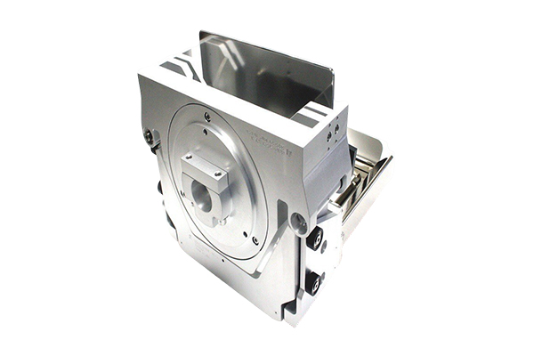
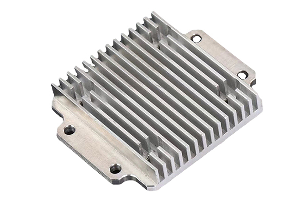
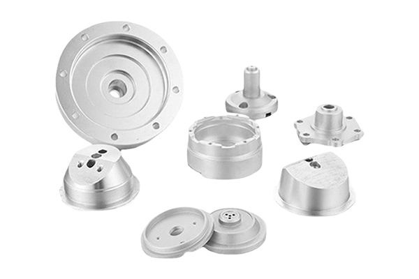
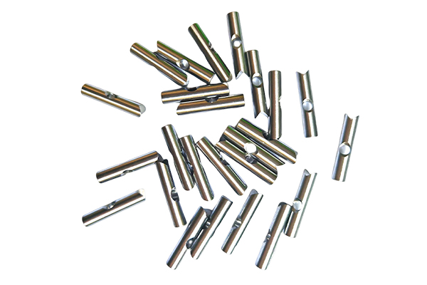
Advanced machining technologies are also essential for producing the miniaturized parts that meet requirements, including precision processing and customization. Laser micromachining, with its high precision and non-contact operation, excels in cutting, drilling, and etching microstructures. It can precisely process submillimeter details, ensuring that each component meets extremely high tolerances. Furthermore, nanofabrication technologies such as electron beam lithography (EBL) and focused ion beam (FIB) are widely used in semiconductor manufacturing to create ultra-fine patterns. Another technology worth noting is additive manufacturing (AM), or 3D printing. Although initially used primarily for prototyping, this technology has now been introduced into production. Using metal powder or polymer filament, 3D printers can build complex three-dimensional structures layer by layer, offering a new manufacturing approach for precision parts processing and customization with complex geometries. This approach not only significantly reduces material waste but also accelerates R&D cycles and reduces costs.
Testing and Quality Control
As the dimensions of precision parts processing and customization decrease, testing and quality control become increasingly challenging. However, this is crucial to ensuring the reliability and safety of the final product. To this end, non-destructive testing technologies such as automated optical inspection (AOI) and computed tomography (CT) are widely used. AOI systems use high-resolution cameras to capture images and analyze them with software to identify any defects. CT scans, on the other hand, can obtain detailed information about a sample's internal structure from all angles, helping to uncover hidden problems. Furthermore, smart sensors and Internet of Things (IoT) technologies are being used to monitor the status of production equipment and product quality in real time. By collecting and analyzing large amounts of data, companies can adjust process parameters promptly to prevent failures, thereby improving the overall efficiency and stability of production lines.
In short, facing the trend of miniaturization of electronic devices, manufacturers of precision parts processing and customization are working hard to overcome challenges through miniaturized design, application of new materials, innovation in precision machining technology, and enhanced testing and quality control. With the continued advancement of science and technology, we believe that these precision parts processing and customization technologies will continue to drive electronic products towards smaller, faster, and more powerful products, providing users with a more convenient and efficient user experience.


